Introduction
In electronics, diodes are essential electronic components that are important in controlling the flow of current in electronic circuits. They are commonly used in various applications, including rectification, signal modulation, and voltage regulation. To fully understand the functionality of diodes, it is important to understand the concepts of forward bias and reverse bias. It's important to know how diodes work to design and improve circuits. Biasing is a key factor that affects how diodes function. This article explores the work of biasing, concentrating on how forward and reverse bias impact diodes. Diode biasing sets the stage for diodes in electronics. It's like giving them the perfect conditions to perform. This behind-the-scenes work ensures diodes, acting as traffic controllers in circuits, function optimally.
Understanding how to bias diodes is important for using them in everyday gadgets like phone chargers and TV remotes. We open diodes when we want them to allow energy and close them when we don't. This basic function is essential for knowing how diodes influence electronic devices, whether by facilitating smooth power flow or creating barriers in circuits.
What is Diode Bias or Biasing?
Diode biasing is generally known as diode bias. It is an important aspect of electronic circuit design that ensures proper functioning and optimal performance of diodes. Biasing involves applying a DC voltage or current to a diode in order to establish its operating point, or bias point. The primary purpose of diode biasing is to set the diode at a specific operating point on its characteristic curve which is known as the diode's current-voltage (I-V) curve. This operating point determines the diode's behavior and enables it to function effectively in a circuit. There are different methods of biasing a diode which are depending on the desired application and circuit requirements. The most common forms of diode biasing include forward biasing, reverse biasing, and zero biasing.
In other words - Before we go to comparing the two types of bias, let's understand what biasing means in electronics. It's like fine-tuning; biasing involves setting specific currents or voltages at different points in a circuit to ensure electronic components work correctly. Simplified, it's the proper adjustment for optimal performance. Within biasing, we have two types – forward bias and reverse bias. Now, think of a diode (PN junction) as a one-way street. It easily lets current flow in one direction but makes it challenging in the other. Simply put, a diode conducts current in one way, following a forward bias. Yet, when the voltage goes in the opposite direction, that's reverse bias. In reverse bias, a standard PN junction diode typically blocks the flow of current, acting like an electronic check valve.
Components Free Worldwide Shipping
Forward Bias vs Reverse Bias
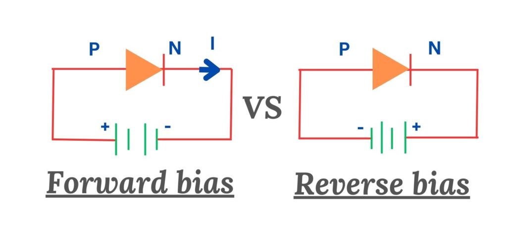
Forward bias is a state in which the positive terminal of a voltage source is connected to the P-side (anode) of a diode, while the negative terminal is connected to the N-side (cathode). Reverse bias, on the other hand, occurs when the positive terminal of a voltage source is connected to the N-side (cathode) of a diode, while the negative terminal is connected to the P-side (anode).
Forward bias vs Reverse bias
Forward Bias In forward bias, the positive terminal of the voltage source is connected to the P-type material of the diode, while the negative terminal is connected to the N-type material. This configuration allows the current to flow through the diode easily, as it reduces the barrier potential. When the voltage across the diode exceeds the forward voltage drop (typically around 0.7 volts for silicon diodes), the diode becomes conductive. Reverse bias, on the other hand, occurs when the positive terminal of the voltage source is connected to the N-type material of the diode, and the negative terminal is connected to the P-type material. In this configuration, the diode acts as an insulator, preventing the flow of current. The voltage applied in reverse bias increases the barrier potential, making it difficult for the current to pass through the diode.
Comparison: Forward Bias vs Reverse Bias
|
|
|
|
|
|
|
|
|
|
|
|
|
|
|
|
|
|
|
|
|
|
|
|
|
|
|
|
|
|
|
|
Forward biasing involves applying a positive voltage across the diode, allowing current to flow through it. This biasing method is commonly used in rectifier circuits, where the diode converts AC input into DC output. Reverse biasing, on the other hand, applies a negative voltage across the diode, causing it to block the flow of current. This biasing method is often used in applications where the diode acts as a protective device or as a voltage reference. Zero biasing, as the name suggests, involves applying zero voltage across the diode. This biasing method is typically used in certain RF (radio frequency) and microwave applications. Proper diode biasing is essential to prevent distortion, ensure stability, and maximize the diode's performance. Incorrect biasing can lead to signal distortion, excessive power dissipation, or even damage to the diode.
The Operation of a Diode
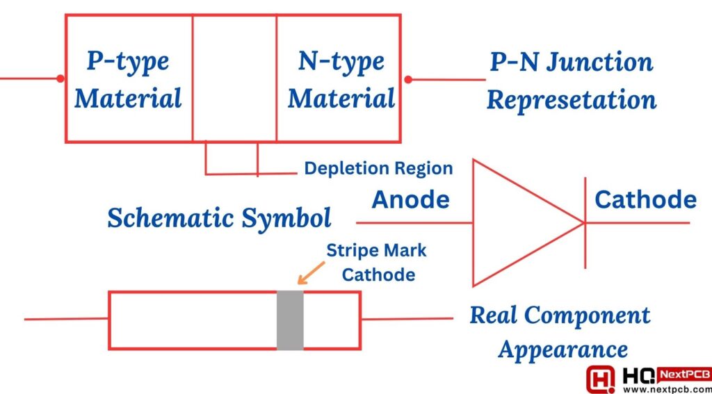
The operation of a diode involves processes rooted in semiconductor physics and quantum mechanics. Specifically, a diode operates as a p-n junction semiconductor, where 'p' represents the positive or anode region, and 'n' represents the negative or cathode region. This configuration is important for diode functionality and is achieved through a process called doping. Doping involves introducing specific materials into the semiconductor to create either an excess of easily displaced electrons (n-type) or an excess of holes ready to absorb electrons (p-type). When these regions are merged to form the p-n junction, they create what is known as the depletion region. The interaction between the positive and negative regions, occurring over extremely short distances, enables the operation of the diode.
The Operation of a Diode
For a diode to function properly, it requires a minimum threshold voltage to overcome the depletion region. Typically, this threshold voltage is around 0.7 volts. The application of reverse-bias voltage may induce a small leakage current, which is generally negligible. However, a significant reverse voltage can lead to a comprehensive electronic breakdown, allowing current to flow in the opposite direction through the diode. The operation of a diode is generally rooted in the physics of semiconductor materials, the creation of p-n junctions through doping, and the establishment of a depletion region. Understanding and controlling these processes are essential for the diode's functionality in electronic circuits.
Diode Functionality and Operation Continued
In a general sense, as diffusion enables electrons to move from the n-type region, they fill the holes in the p-type region. This process leads to the formation of negative ions in the p-type region, leaving positive ions in the n-type region. The electric field's direction governs this action, influencing the overall electrical behavior. The outcome is dependent on the applied voltage, known as biasing. In the context of a typical p-n junction diode, there exist three biasing conditions and two operational regions. These three biasing conditions include:
Forward Bias : When a diode is in forward bias, the positive terminal of the voltage source is connected to the anode (P-side) of the diode, and the negative terminal is connected to the cathode (N-side). This creates a forward current flow through the diode, allowing it to conduct electricity. In this state, the diode has a low resistance and behaves like a closed switch. Forward biasing a diode allows it to perform its intended function, such as emitting light in an LED or rectifying AC voltage in a rectifier diode. It is important to note that the forward voltage drop across a diode is typically around 0.7 volts for silicon diodes and 0.3 volts for germanium diodes.
Reverse Bias : In reverse bias, the positive terminal of the voltage source is connected to the cathode (N-side) of the diode, and the negative terminal is connected to the anode (P-side). This configuration creates a reverse current flow, which prevents the diode from conducting electricity. In this state, the diode has a high resistance and behaves like an open switch. Reverse biasing a diode is useful for applications such as blocking unwanted current flow or protecting sensitive electronic components from excessive voltage. It is important to note that a diode can withstand a certain amount of reverse voltage, known as the breakdown voltage, before it starts conducting in reverse bias.
Zero Bias: Zero biasing involves applying zero voltage across the diode. This biasing method is typically used in certain RF (radio frequency) and microwave applications.
Forward Biasing Versus Reverse Biasing and their Variances
The distinction between forward biasing and reverse biasing is important in understanding the operation of diodes and other semiconductor devices. Let's explore the key differences between the two:
In forward biasing, the positive terminal of the voltage source is connected to the P-type material of the diode, while the negative terminal is connected to the N-type material. This configuration allows current to flow through the diode easily, as it reduces the barrier potential. When the voltage across the diode exceeds the forward voltage drop (typically around 0.7 volts for silicon diodes), the diode becomes conductive. Forward biasing is commonly used in rectifier circuits, converting AC input into DC output. On the flip side, in reverse biasing, we connect the positive terminal of the voltage source to the N-type material of the diode, and the negative terminal is connected to the P-type material. This setup acts as an insulator, preventing the flow of current. The voltage applied in reverse bias increases the barrier potential, making it difficult for current to pass through the diode. Reverse biasing is often utilized in applications where the diode acts as a protective device or voltage reference.
Variances: Looking at the variances between the two:
- Voltage Polarity: Forward biasing has a positive voltage applied to the anode (+), while reverse biasing applies a negative voltage to the anode (-).
- Current Flow: Forward biasing allows significant current flow, while reverse biasing allows minimal current flow.
- Diode Conductance: Forward biasing results in high conductance, while reverse biasing leads to low conductance.
- Barrier Potential: Forward biasing reduces the barrier potential, aiding conduction, whereas reverse biasing increases the barrier potential, hindering flow.
- Diode Behavior: In forward bias, the diode acts like a closed switch, facilitating current flow. In reverse bias, it acts like an open switch, blocking the current.
|
|
|
|
|
|
|
|
|
|
|
|
|
|
|
|
|
|
|
|
|
|
|
|
|
|
|
|
Conclusion
In conclusion, understanding the concepts of forward bias and reverse bias is essential for comprehending diode functionality in electronic circuits. The article has covered the fundamental aspects of diode biasing, exploring how the positive and negative terminals of a voltage source influence the behavior of diodes. We discussed the operation of a diode, delving into the processes rooted in semiconductor physics and the creation of p-n junctions through doping. Furthermore, the article highlighted the variances between forward biasing and reverse biasing, emphasizing their impact on diode conductance, barrier potential, and overall behavior.
The differences in voltage polarity and current flow were outlined to provide a comprehensive understanding of the distinct roles each bias plays in electronic circuits. Ultimately, this exploration into forward and reverse bias, along with their variances, contributes to a foundational knowledge of diode functionality. This knowledge is important for engineers and enthusiasts alike, enabling them to design and optimize electronic circuits for various applications, from rectification and voltage regulation to signal modulation and protection against voltage surges.
Comment