Nowadays in this electronics and technology world, ICs are of capital importance. Almost every piece of electrical equipment that we need includes integrated circuits, from computers, phones and smartphones to home appliances, TVs and cars. Nevertheless, we can mention many different kinds of integrated circuits which have different purposes. In this paper, we distill the three categories of integrated circuits - digital, analog, and mixed-signal ICs - and their important aspects will be mentioned subsequently.
What is Integrated Circuit?
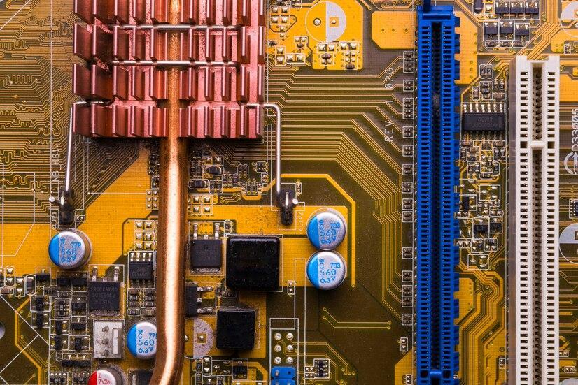
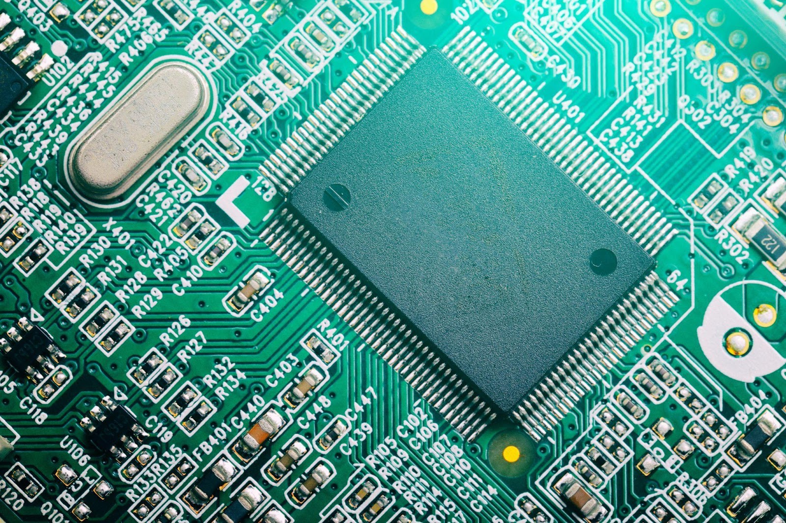
An integrated circuit (IC) or a microchip is a miniaturized electronic circuit, which is manufactured by the process of photolithography; and ICs are usually made up of very tiny resistors, capacitors, and transistors, etched on a semiconductor substrate made of either silicon or germanium. The IC chip is the device of integration of the entire circuit into a chip with a semiconductor material which usually is silicon as the base material.
ICs are built on silicon wafers or chips that have not only thousands but also millions of tiny resistors, transistors and other elements of a circuit. These items or beings are interrelated to form full circuits. Circuit might be reconfigurable which can change its functionality even after manufacturing.
Integrated circuits, being the basis of these advanced digital technologies, offered more convenience in our lives and helped technologies to work flawlessly. Modern devices like computers, smartphones, appliances and cars that make up the world around us could not be manufactured without integrated circuits miniaturizing entire systems into tiny, yet high-performance silicon chips. ICs classification can be made based on the purpose of their application. In this article, we will get familiar with the main classes of integrated circuits.
Digital Integrated Circuits
Digital integrated circuits or digital ICs are those that process digital or discrete signals - signals that have clear high and low values represented by 1s and 0s in binary form. These ICs perform logic, arithmetic, coding/decoding and storage functions through combinations of switches (transistors). Common examples of digital integrated circuits include:
- Microprocessors: The CPU and the memory which control the operation of computers and other electronic devices are also made from silicon. IC Chip that has combined the ALU, control unit, registers, memory, and bus connections by the microprocessors. From Intel and AMD CPUs to other popular microprocessor ICs, the industry continues to advance.
- Microcontrollers: Self-contained systems with a processor, memory and input/output capabilities built into a single IC. Common in embedded systems and devices that require some level of intelligent control and processing. Microchip and Texas Instruments provide many varieties of microcontroller ICs.
- Memory ICs: Responsible for storing digital data and program instructions. Different types include RAM, ROM, flash memory, hard drives, and more. Memory capacity keeps increasing as new generations are introduced. Samsung, Micron, and Hynix are leading memory IC manufacturers.
- Logic Gates: Primary components of logic gates that realize logical operations of AND, OR, NOT on binary inputs. Some common logic gates include transistors, NAND gates, NOR gates, etc.
- Programmable Logic Devices: Digital ICs with programmable digital ICs, which are reprogrammable and contain configurable logic blocks and interconnects to implement custom logic functions and systems. e.g. the FPGAs from Intel/Altera and Xilinx.
- Interface/Communication ICs: Facilitate data transmission between digital systems and components. Interface ICs include USB, Ethernet, WiFi chips, display drivers, audio codecs and more.
The key attribute of digital integrated circuits is that they manipulate discrete voltage levels to represent information as binary digits. Any system involving computation, storage or digital logic/control relies on digital ICs as fundamental building blocks. Digital IC design and fabrication continue advancing Moore's Law allowing more transistors to be integrated.
Analog Integrated Circuits
In contrast to digital ICs, analog integrated circuits or analog ICs process continuous, real-world analog signals like voltage, current or sound waves. Rather than discrete values, analog signals can vary continuously over a range of values. Common examples of analog integrated circuits are:
- Operational Amplifiers (Op-Amps): Universal building block for analog circuits providing voltage amplification, comparison and other functions. Widely employed in instrumentation, control systems and signal processing. Texas Instruments, Analog Devices produce popular op-amp ICs.
- Audio/Video Chips: Analog ICs that encode/decode analog audio and video signals. Include sound cards, video/graphics controllers, TV tuners, codecs etc. Nvidia, AMD, and Qualcomm supply analog multimedia SoCs.
- Sensor Interface ICs: Read signals from analog sensors like temperature probes, pressure gauges, position/motion sensors. ADCs convert sensor readings to digital for processing.
- Power Management Chips: Regulate voltages for internal circuits and components from batteries or power adapters. Maintain stable voltages despite load variations and fluctuations. ON Semiconductor, Maxim Integrated focus on power ICs.
- Oscillators: Clock signals and timing circuits generating periodic waveforms. Include crystal oscillators in watches/clocks and resonant circuits in radios. Epson, NXP Semiconductor offer oscillator ICs.
Analog circuits demand tight matching and tracking of current, voltage and timing. Even minor tolerances can degrade analog IC performance. Advanced precision fabrication techniques are essential for building high-end linear and mixed-signal ICs.
Mixed-Signal Integrated Circuits
As the title indicates, the mixed-signal ICs, also known as Mixed-signal integrated circuits, come with the combination of both analog and digital circuitry onto a single chip. Therefore, it facilitates encapturing of interfacing between analog real phenomena and digital systems for control, analysis, and communication:
- Microcontrollers with Analog-to-Digital Converters (ADCs): Microchip PIC, Arduino boards with onboard ADCs to accept analog inputs. Facilitate building embedded systems interfacing sensors and actuators.
- Digital Signal Processors: Combine DSP algorithms and serial/parallel ADCs for communication, audio, instrumentation and embedded applications. Popular DSP chips from Analog Devices, Texas Instruments.
- CMOS image sensors: Integrate photodiodes, analog gain/sampling circuits and ADCs in cameras. Offer higher quality images than traditional CCDs. Sony, Samsung lead in CMOS image sensor ICs.
- Touch Controllers: Mixed-signal touchscreen chips featuring analog touch sensing and digital reading/response capability. Used in cellphones, tablets, monitors, POS devices etc.
- Set-Top Box Chips: Analog tuners, demodulators along with digital decoders/processors enable streaming multimedia content. Supply by Broadcom, Intel and others.
- Audio Amplifiers: Drive speakers combining Class-D analog output power stages and digital signal processing cores. Enable smaller audio equipment. Texas Instruments dominates analog/digital audio.

Mixed-signal design presents myriad challenges due to interactions between analog and digital blocks. Noise coupling, power supply variations, timing issues require specialized expertise and tools. However, it enables single-chip solutions integrating sensors, control and processing functionality.
Applications of Digital, Analog and Mixed-Signal ICs
Now that we have explored the types and examples of integrated circuits, let's examine some common applications that utilize digital, analog and mixed-signal ICs:
Computers and Servers: Utilize digital microprocessors, memory chips, logic gates, interface ICs while also incorporating ADC/DACs and mixed-signal chips like graphics cards and multimedia controllers.
Smartphones and Tablets: The majority is digital including applications processors, storage and cellular modems. However, include mixed-signal SoCs for touchscreens, cameras, audio in addition to sensors interfaced by analog ICs.
Automotive Electronics: A combination of digital engine/transmission control units, infotainment and driver-assist ICs. Also, analog sensor interfaces, power management and wireless communication ICs. ADAS systems are predominantly mixed-signal.
Home Appliances: Mostly employ microcontrollers and specialized digital and mixed-signal ICs for appliance-specific functions like washing machines, dishwashers, air conditioners and refrigerators with humidity/temperature sensors.
Industrial Equipment: Leverage digital PLCs, motor drives and logic controllers. Also contains analog measurement and feedback circuits. Robotic systems contain both digital control and analog servo motor/positioning hardware.
Medical Equipment: Range from fully digital defibrillators, CT/MRI machines to predominant analog devices like ECG/EEG monitors, ultrasound scanners with digital elements. Hearing aids represent highly complex mixed-signal devices.
Audio/Visual Systems: While high-end AV amps, receivers contain powerful DSP chips, they require mixed-signal interfaces and analog output stages. Digital camera image sensors get aid from analog pixel arrays and ADCs.
Wireless Infrastructure: Base stations rely on mixed-signal RF/microwave front-ends for transmission/reception combined with digital signal/protocol processors. WiFi chips similarly integrate analog RF and digital MAC/network cores.
Given the diversity of applications and usage models, all categories of integrated circuits - digital, analog and mixed-signal find widespread deployment. As technology evolves, IC design is moving towards system-on-chip solutions combining previously discrete functions on a single mixed-signal die. This allows greater miniaturization, lower power consumption and simplified manufacturing for electronic products.
Integrated Circuit Fabrication Process
Now that we understand the basic functioning and applications of different IC types, let us briefly examine the fabrication process behind manufacturing these chips:
- Wafer Creation: High-purity silicon ingots are created using the Czochralski process and sliced into wafers around 300mm in diameter. Wafers form the base substrate for all ICs.
- Oxidation: Silicon dioxide is grown on the wafer surface by heating in an oxygen environment. This forms the starting dielectric material for building transistors.
- Photolithography: Photoresist polymer is spun and baked on the wafer. Masks are used to expose patterns via UV light through a photomask. Developers etch exposed resistors.
- Etching: Through openings in the photoresist layer, patterns are transferred to underlying oxide or polysilicon using wet/dry etching. Forms individual circuit elements.
- Doping: High-energy dopant atoms like boron or phosphorus are implanted and diffused into silicon to alter conductivity. Defines transistors, resistors.
- Metallization: Barrier materials and thin films of aluminum or copper are deposited and patterned to form wiring layers connecting components.
- Packaging: Wafers are diced, dies are attached to lead frames or substrates, bonded with gold wires, and encapsulated with plastic molding in packages.
- Testing: Automated test equipment applies voltage and tests functionality of packaged chips to separate good versus defective ICs.
The above wafer fabrication processes involve complex photolithographic techniques repeated many times with tight process variation control. Billions of transistors are arranged in 3D stacks through multiple wiring layers to build dense integrated circuits.
Challenges and Trends in IC Design and Manufacturing
While integrated circuit technology has progressed tremendously over the years to enable advanced electronics, there are ongoing challenges as well as emerging trends in IC design and fabrication:
- Continuous Scaling: Shrinking transistors and circuit elements below 5nm according to Moore's Law requires new materials and 3D architectures. Quantum tunneling, power density rise concerns loom.
- Yield and Reliability Issues: Minimizing defects and improving mean time between failures becomes crucial as billions of components pack into tiny die areas. Process noise affects analog/RF chip yields.
- Cost of Manufacturing: Setting up leading-edge fabs and photolithography equipment exceeding $10 billion drives efforts to maximize wafer volume production.
- Mixed-Signal Integration: Integrating analog, digital and RF onto a single substrate requires balancing performance with noise isolation and matching.
- Design Complexity: SoC chips with ten billion transistors need massive parallel EDA tools and methodologies to handle design rules, verification for error-free functionality.
- Heterogeneous Architectures: Mixing CPU, GPU, digital signal processor cores on a single die calls for new interconnect fabric and programming models.
- Emerging Technologies: 3D stacking, carbon nanotube FETs, spintronics, and neuromorphic circuits represent future alternatives to conventional CMOS scaling.
- Customization: Demand is rising for niche application-specific ICs versus more generalized solutions due to Internet of Things proliferation.
To overcome challenges, the IC industry focuses on new materials, 3D monolithic stacking, customized chips, heterogeneous computing and design automation advances moving forward. Integrated circuits will keep revolutionizing technology as their capabilities continue doubling every couple of years through collaborative research and manufacturing investments.
Emerging Integrated Circuit Technologies
While CMOS-based digital and mixed-signal ICs dominate today's electronics landscape, researchers are actively exploring several promising emerging IC technologies that could shape the future:
3D Integrated Circuits
As traditional silicon scaling reaches its physical limits, 3D chip stacking has become an important avenue for extending Moore's Law. 3D ICs involve making vertical connections between multiple active circuit layers to dramatically increase transistor density. There are a few main approaches:
- Through-Silicon Vias (TSVs): Vertical holes are etched through a wafer and filled with conducting material like copper to connect layers. Allows stacking up to 5 layers currently with Through-Silicon Reach (TSR) and monolithic 3D taking it further.
- Die/Wafer Stacking: Discrete memory or logic dies/wafers are vertically stacked and interconnected using micro-bumps and Redistribution Layers (RDLs). Widely adopted in high-end mobile phones packing multiple processor chips.
- Monolithic 3D: Separate device layers are built atop each other on a single crystal silicon substrate. Each layer can contain its own standard CMOS transistors. Potential to stack 10-100 layers and achieve 1000x density gains.
Stacked 3D ICs bring benefits of heterogeneous integration by combining specialized circuits together. Challenges include thermal issues, RDL reliability and design complexity associated with vertical wiring. Still early in development commercially but demonstrates the possibility of continuing Moore's scaling path vertically.
Carbon Nanotube FETs
By replacing silicon as the semiconductor channel material, carbon nanotubes (CNTs) - rolled up graphene sheets just 1nm wide - promise to enable ultra-fast, ultra-low power ICs. They function similarly to graphene transistors but have a bandgap suitable for digital logic. Some key advantages of CNTFETs include:
- Ballistic transport: Electrons can travel at near-light speed through them with little scattering providing terahertz switching capabilities.
- Higher current density: Much higher than silicon allowing for less area usage and interconnects.
- Ambipolar characteristics: Act as both NMOS and PMOS devices in a single CNT enabling novel circuit designs.
Research prototypes have shown CNTFET ICs outperforming silicon. However, issues remain around batch production of uniform semiconducting CNTs and integration challenges into foundries. Once solved, CNT ICs could surpass the performance of silicon by orders of magnitude.
Spintronic Integrated Circuits
- Traditional electronics are based on the charge of electrons but not their intrinsic spin property. Spintronic devices use electron spin states ("up" or "down") along with charge to offer non-volatility, enhanced functionality and lower power operation. Some spintronic technologies include:
- Spin Transfer Torque MRAM (STT-MRAM): Combines RAM and non-volatile magnetic storage in a single component. Far faster and denser than NAND flash. Samsung commercialized mobile SoCs.
- Spin Logic Devices: Novel "spin transistors" have been proposed based on spin precession/manipulation for ultra-low power Boolean and non-Boolean logic operations.
- Racetrack Memory: Data is stored as domain walls between magnetic regions in nanowires that can be moved and stored at higher densities than NAND.
While still early, spintronics opens a new paradigm beyond charge transport that can potentially replace CMOS. Interfacing spin circuits with standard transistors remains under active research.
Quantum-dot Cellular Automata
As the name suggests, quantum-dot cellular automata (QCA) aims to build computing blocks from quantum dots - nanoscale particles holding single electrons or nuclear spins. Individual dots can represent classical bits as either electron presence ("1") or absence ("0"). Complex circuits are self-assembled from arrays of interconnected quantum dots switchable via electrostatic forces:
- Inherently low power as switching relies on quantum tunneling and Coulomb forces rather than traditional current flow.
- Can perform parallel computations based on how electrons settle in QD lattice due to inter-dot electrostatic interactions.
- Possible to fabricate dot cells just 5-10nm in size enabling extremely dense circuits.
While fascinating, QCA technology faces daunting quantum control as well as integration challenges making it very long-term. Progress is ongoing to better understand defects, thermal stability and logic design rules for prospective post-CMOS quantum computing.
Components Free Worldwide Shipping
Neuromorphic Integrated Circuits
Taking inspiration from biological brains, neuromorphic or neural network-inspired chips aim to maximize parallelism, learning capability and low-power operations. They mimic neural signaling between artificial neurons and synapses:
- IBM's "TrueNorth" chip contains 5.4 billion transistors functioning as 1 million spiking neurons communicating via 256 million synapses consuming only 70mW power. Used for AI inference tasks.
- Intel's "Loihi" chip contains over 130,000 digital neuromorphic cores on a single die interconnected as a neural network. Learns online through Spiking Deep Learning algorithms.
- Qualcomm's Zeroth chip integrates AI processing directly on sensor hardware for applications like computer vision and augmented reality.
While digital implementations currently, longer-term analog memristive and spintronic devices may better emulate true biological synaptic plasticity and weighted connections for highly energy-efficient neuromorphic computing. Area of active research bridging neuroscience, nanoelectronics and machine learning algorithms.
In summary, while CMOS scaling continues, advanced 3D stacking, novel materials like carbon nanotubes and spintronic/quantum devices provide exciting potential pathways to extend Moore's Law for decades to come. Emerging technologies promise radical improvements in performance, power and functionality beyond what is achievable with silicon alone. Commercial adoption depends on overcoming key technological hurdles.
Comment